|

Memoirs
Created 28.10.2008
Updated 25.3.2022
|
|
BOOKS
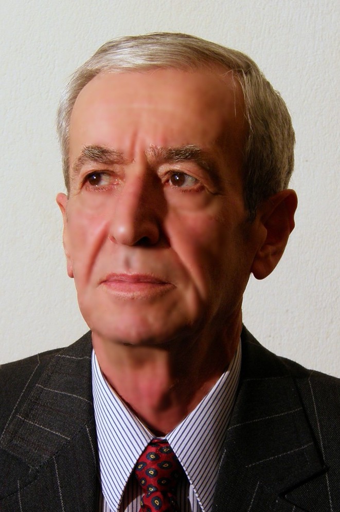
PETAR CHRISTOV PEYKOV
private collection
|
|
Biography
Field of research interests: Semiconductors, microelectronics, sensors, nanotechnologies, numerical and statistical modeling of semiconductor devices and technologies, data mining
Year and place of birth: 1939, Sofia
Education Petar Peykov graduated from Faculty of Physics, Sofia University “St. Kl. Ohridsky” in 1966. In 1973, he obtained PhD in Physics and Mathematics from the Institute of Semiconductors, Ukrainian Academy of Sciences, Kiev, Russia
Career: Institute of Physics, BAS - physicist; Institute of Solid State Physics, BAS - research associate; Institute of Microelectronics, Ministry of Electronics – 1-st deputy director, senior research assistant of 2nd degree; Universidad Autуnoma de Puebla, Mexico – visiting professor; Instituto Nacional de Astrofнsica, Уptica i Electrуnica – senior researcher category “C”; SNI – researcher level II; Faculty of Physics, Sofia University – physicist
Teaching experience: He was lecturer more than 20 years in 8 different courses as: part – time lecturer in the Faculty of Physics, Sofia University, visiting professor in the Universidad Autуnoma de Puebla, Mexico and in the Instituto Nacional de Astrofнsica, Уptica i Electrуnica, Mexico
Publications Over 123 scientific articles, 2 monograph, 9 Bulgarian patents and 2 in Russia
P. Peykov, Effects of some factors on pulse MOSC-t measurements, Доклади на БАН, 28, с. 1323 (1975)
P. Peykov, Photoelectric properties of MOS structures non-equilibrium conditions, Доклади на БАН, 28, с. 1319 (1975)
P. Peykov, Discharging of MNOS structures with thick oxide at higher temperatures, Доклади на БАН, 29, с. 175 (1976)
P. Peykov, On the nature of the negative charge in MNOS structures, Доклади на БАН, 29, с. 171 (1976)
P. Peykov, A. Vitkov, On the nature of the negative charge in MNOS structure, Comptes Rendus de l'ABS, 29(2) p. 171-173 (1976)
P. Peykov, A. Vitkov, M. Kaminova, G. Beshkov, V. Lazarova, Discharging of MNOS structures with a thick oxide at higher temperature, Comptes Rendus de l'ABS, 29(2) p. 175-177 (1977)
P. Peykov, The influence of process induced defects in the Si on surface charge in MOS structures, Thin solid films, 48(3) p. (1978)
|
|
|
